Have at look at my desktop with windows VISTA inspirat theme pack.

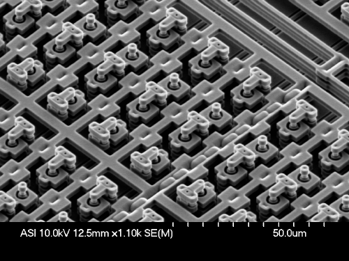
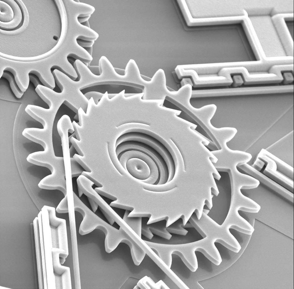
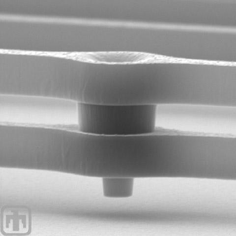
Automotive: the first high volume application
After spending about 25 years in the lab, however, it was the automotive industry which first commercially embraced MEMS devices in the '90's as airbag accelerometers, recognizing the benefits of MEMS devices' small size, relative low cost and high degree of sensitivity.
Early airbags required the installation of several bulky accelerometers made of discrete components mounted in the front of the car, with separate electronics near the airbag (at a cost of over $50). Today, because of MEMS, the accelerometer and electronics are integrated on a single chip at a cost of under $10. The small size (about the dimensions of a sugar cube) provides a quicker response to rapid deceleration. And because of the very low cost, manufacturers are adding side impact airbags as well. The sensitivity of MEMS devices is also leading to improvements where size and weight of passengers will be calculated so the airbag response will be appropriate for each passenger.
There are many other automotive applications for MEMS either in use now or coming soon, including fuel pressure sensors, air flow sensors, tire pressure sensors with automatic built-in tire pumps, “smart” sensors for collision avoidance and skid detection, “smart” suspension for sport utility vehicles to reduce rollover risk, automatic seatbelt restraint and door locking, vehicle security, headlight leveling, and navigation.
MEMS come of age
Another wide deployment of MEMS is their use as micronozzles that direct the ink in inkjet printers. They are also used to create miniature robots (micro-robots) as well as micro-tweezers, and are used in video projection chips with a million moveable mirrors.
MEMS have been rigorously tested in harsh environments for defense and aerospace where they are used as navigational gyroscopes, sensors for border control and environmental monitoring, and munitions guidance. In medicine they are commonly used in disposable blood pressure transducers and weighing scales.
Out of these practical experiences have grown a raft of other applications which are quickly approaching everyday use. For example, engineers are utilizing the ability of MEMS devices to collectively assemble information and applying it to “smart roads.” Smart roads would be covered with millions of MEMS sensors. The sensors would act as a blanket of information, gathering and transmitting data about road conditions to people charged with maintaining them. Problems with roadways would be detected and repaired before they became serious. These smart roads could also send information to cars equipped with Global Positioning Devices, informing the on-board computer of road hazards, accidents, and traffic. Another safety application includes the detection of black ice on roadways and the development of windshields with automatic glare resistance.
Other arenas into which MEMS are moving include package shipping, where MEMS shock sensors would rest inside packages to monitor time and any type of damage that may occur while the package is in transit. One commercial application that is coming to market within months is a compact skin analysis unit for medical and consumer use, including department store cosmetics counters and pharmacies. This tool will contain small sensor-based units to analyze the physical and chemical properties of skin surfaces.
An additional and significant growth area for MEMS today is in telecommunications where the technology is being used for wireless applications as well as in optical networks.
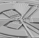
Like ICs, the structures are developed in thin films of materials. The processes are based on depositing thin films of metal or crystalline material on a substrate, applying patterned masks by photolithographic imaging, and then etching the films to the mask. In effect, a sacrificial layer is introduced – a material which keeps other layers separated as the structure is being built up but is dissolved in the very last step allowing selective parts of the structure free to move.
This use of established “batch” processing of MEMS devices, similar to volume IC manufacturing processes, eliminates many of the cost barriers that inhibit large scale production using other less proven technologies. Although MEMS fabrication may consist of a multi-step process, the simultaneous manufacture of large numbers of these devices on a single wafer greatly reduces the overall per unit cost.
Making the transition: from prototype to manufacture
Prototyping is integral to the process, however. An initial device is produced that can be characterized, measured, and optimized for performance and high volume manufacture. A key challenge can be the leap from prototype to high volume manufacture – a transition that sometimes requires considerable modifications. This requires the availability of broad-based design and process expertise (not just application experience), as well as appropriate software tools that can automatically provide process customization. CAD tools are crucial to a cost and time-effective process. Previously developed internally, there are now several commercially available CAD packages that guide engineering teams through component design, system design, and analysis.
It's important to note that MEMS manufacturing technology is not a uniform science but rather a combination of design techniques and knowledge of materials, process, and applications. Processes may vary considerably. For example, the techniques used for wireless may not work at all for the development and production of optical communications devices. Further, although MEMS and IC manufacturing is based on photolithographic etching, in many cases the processes and/or materials may not be compatible. It's interesting to note that gold, which is required in the manufacture of optical MEMS, will contaminate an IC batch.
There are three general approaches to the fabrication of MEMS: surface micromachining, bulk micromachining, and LIGA (lithography, plating, molding).
Surface micromachining is a process based on the building up of material layers selectively remaining or removed by continued processing. The bulk of the substrate remains untouched.
In bulk micromachining, large portions of the substrate are removed to form the desired structure. Structures with greater heights can be formed because thicker substrates can be used. The bulk micromachining process is a key fabrication method used for MEMS-based photonic switching in the high-growth optical and wireless markets.
LIGA processes combine IC lithography and electroplating and molding to obtain depth. Patterns are created in a substrate and then electroplated to create 3D molds. These molds can be used as the final product, or various materials can be injected into them. This process has two advantages. Materials other than silicon can be used (e.g. metal, plastic) and devices with very high aspect ratios can be built.
The fabrication process is usually a structured sequence of THREE BASIC PROCESSES:
1. Deposition
Deposition is a key building block in that it is the ability to deposit thin films of material (for subsequent local etching). MEMS deposition technology is classified in two groups:
Depositions resulting from chemical reactions: chemical vapor deposition, electrodeposition, epitaxy, and themal oxidation. These processes exploit the creation of solid materials directly from chemical reactions in gas and/or liquid compositions or with the substrate material. The solid material is usually not the only product formed by the reaction. Byproducts can include gases, liquids and even other solids.
Depositions resulting from physical reaction: physical vapor deposition, casting. The material deposited is physically moved on to the substrate (a chemical byproduct is not created).
2. Etching
In order to form a functional MEMS structure on a substrate it is necessary to etch the thin films previously deposited and/or the substrate itself. In general, there are two classes of etching processes:

To make a donation
You can also ask for those original wonderful lively pictures that my friends click by making a small donation to us


