A Very Large Scale Integrated (VLSI) circuit is a conglomerate of a large number of practically identical, very reliable switches interconnected to express a computing function. The relentless miniaturization of the components that comprise an Integrated Circuit (IC) which has occurred over the last 30 years has been one of the key ingredients to improving performance while reducing cost by a factor of 100,000. Ultimately, it will become uneconomical to produce reliable transistors through miniaturization, however. The figure shows a cross-section through a 35nm gate length MOSFET, a "nano - transistor", obtained using high resolution Transmission Electron Microscope (TEM). The channel length is only about 100 silicon lattice sites long. An enlargement of the channel region delineated by red on the left is shown on the right. The regular array of atoms show in the lower portion of the lattice image corresponds to the single crystal silicon substrate. The gate oxide thickness estimated from the image is only about 1.0nm. The sensitivity to atomic variables is not welcomed by manufacturing
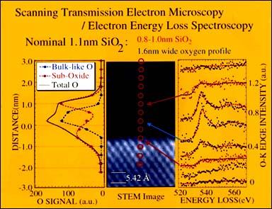
To achieve high performance and high drive current with the low power supply voltage required to minimize power dissipation, the thickness of the gate oxide in sub-100nm CMOS technologies must scale to less than 2nm. However, high resolution Scanning Transmission Electron Microscopy (STEM) used in conjunction with Electron Energy Loss Spectroscopy (EELS) reveals an ultimate physical lower limit to the thickness of about 0.7nm. The figure shows a STEM image of a typical polysilicon/SiO2/silicon gate stack in MOSFET. It shows a regular array of silicon atoms in the substrate, which terminate at the SiO2/Si interface. The chemical constituency of the gate stack and the bonding can be probed by analyzing the energy loss of the transmitted electron beam. We find that a nominally 1.1nm thick oxide has 0.8-1.0nm of bulk SiO2 (blue dashed line) with flanking sub-oxide layers above and below the oxide which are 0.5nm and 0.3nm wide respectively (red dashed line). When the sub-oxide layers coincide, the tunneling barrier associated with the oxide collapses.