Thursday, October 13, 2005

What is CDMA technology?


The world is demanding more from wireless communication technologies than ever before as mre people around the world are subscribing to wireless. Add in exciting Third-Generation (3G) wireless data services and applications - such as wireless email, web, digital picture taking/sending, assisted-GPS position location applications, video and audio streaming and TV broadcasting - and wireless networks are doing much more than just a few years ago.

This is where CDMA technology fits in. CDMA consistently provides better capacity for voice and data communications than other commercial mobile technologies, allowing more subscribers to connect at any given time, and it is the common platform on which 3G technologies are built.

CDMA is a "spread spectrum" technology, allowing many users to occupy the same time and frequency allocations in a given band/space. As its name implies, CDMA (Code Division Multiple Access) assigns unique codes to each communication to differentiate it from others in the same spectrum. In a world of finite spectrum resources, CDMA enables many more people to share the airwaves at the same time than do alternative technologies.

The CDMA air interface is used in both 2G and 3G networks. 2G CDMA standards are branded cdmaOne and include IS-95A and IS-95B. CDMA is the foundation for 3G services: the two dominant IMT-2000 standards, CDMA2000 and WCDMA, are based on CDMA.

cdmaOne: The Family of IS-95 CDMA Technologies
cdmaOne describes a complete wireless system based on the TIA/EIA IS-95 CDMA standard, including IS-95A and IS-95B revisions. It represents the end-to-end wireless system and all the necessary specifications that govern its operation. cdmaOne provides a family of related services including cellular, PCS and fixed wireless (wireless local loop).

CDMA2000: Leading the 3G revolution
CDMA2000 represents a family of ITU-approved, IMT-2000 (3G) standards and includes CDMA2000 1X and CDMA2000 1xEV technologies. They deliver increased network capacity to meet growing demand for wireless services and high-speed data services. CDMA2000 1X was the world's first 3G technology commercially deployed (October 2000).

CDMA Deployments
CDMA is the fastest growing wireless technology and it will continue to grow at a faster pace than any other technology. It is the platform on which 2G and 3G advanced services are built.

Wednesday, October 12, 2005

Dont spoil the life of innocent children for the sake of WAR


This is an artists sattarical painting on American's occupation of Iraq.

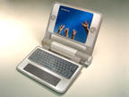
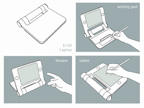
LAPTOP @ $100


Yeah this gonna become true because the researchers at MIT have made a prototype laptop and this will be market by 2006-jan.
This is mainly designed forthe sake of students and will serve them in various ways!
It needs only a small amt of charge.
do have a look at the pics of this middle class frendly lap top

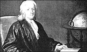
Newton papers revealed:Gravity theory


Sir Isaac Newton, a physicist and mathematician, laid the foundations for modern science.
His theories on mathematics, optics and gravity have shaped our thinking for over 300 years.
The mass of papers he left after his death in 1727 were divided into two main collections, one of which was presented to the university a hundred years later

Monday, October 10, 2005

ROBOTIC FISH


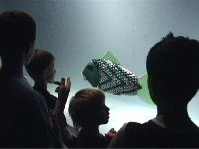
There may be a different fish to see for every day of the year at the London Aquarium at County Hall, but now there's a new variety that has never swum any of the world's oceansThree stunningly beautiful robotic fish have been created with jewel-bright scales and sinuous, astonishingly life-like movements.


They have been produced by Professor Huosheng Hu and his human-centred robotics team of the Department of Computer Science at the University of Essex.

Professor Hu's team have been working with the London Aquarium for three years to develop a biologically inspired robotic fish which mimic the undulating movement of nature's fish species - aiming for the speed of the tuna; the acceleration of a pike, and the navigating skill of the eel.

The robotic fish have sensor-based controls and autonomous navigation capabilities – they can find their own way around the tank safely, avoiding the objects, and react to their environment. The results of years of painstaking work can now been seen in freshwater tanks next to the London Aquarium's Atlantic tanks.

Professor Hu is an expert in the field of robotics and was the mastermind behind the Essex robotic football team who won the 3rd prize in the RoboCup simulation league in 1999. The robotics group at Essex is one of the largest in the UK and is at the cutting edge of research into human-centred robotics.

According to Professor Hu, the aim of the project is to bring the public in direct contact with robots, increasing their understanding of science and technology. "This work has many real-world applications including seabed exploration, detecting leaks in oil pipelines, mine countermeasures, and improving the performance of underwater vehicles."

The Aquarium's marine experts have worked with the robotics team to share their knowledge of the behaviour and movement of a wide variety of fish, and have provided the facilities within the Aquarium for the robotics team to study many species in great detail.

"Our robotic fish are really wonderful to look at and very entertaining," commented Foster Archer, director of the London Aquarium. "It's amazing how beautiful and graceful their movements are - they're going to be incredibly popular with our visitors."

ALSO CHECK OUT this link for the actual article:
http://www.london-se1.co.uk/news/view.php?ArtID=1774

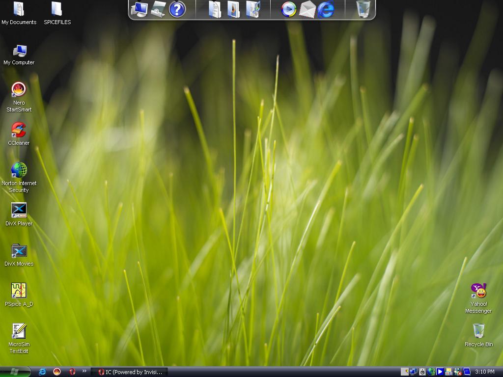
WINDOWS VISTA SCREEN-SHOT(theme)


Have at look at my desktop with windows VISTA inspirat theme pack.

Thursday, October 06, 2005

Nano Chips Require Nano Packaging


Information technology (IT) is more than a trillion dollar industry. It includes hardware, software, services and applications. Contrary to the perception, the hardware accounts for better than two thirds and the single most important building block of this hardware, of course, is semiconductor devices such as CMOS, Ga -As, Si- Ge, Silicon- on- insulator for a variety of digital, RF, analog and optoelectronic applications. The total worldwide annual market for these devices is about $150 - 200 B. These devices, the technology for which is at the threshold of Nano scale (100nm), are typically fabricated into wafers as big as 300 mm in diameter and are subsequently diced into individual ICs. They are then packaged, tested, and burned into individual IC devices ready to be surface mount bonded onto system level boards. The total number of ICs produced in year 2000 was about 375B units, each packaged at some cost, typically $00.01U.S. per I/O. The total packaging market, which includes IC Packaging as well as system's packaging, is almost as big as the semiconductor market, together accounting for 25% of IT.

Friday, September 30, 2005

nano tube transistors

Yorktown Heights, N.Y. - May 20, 2002 - IBM today announced it has created the highest performing nanotubes transistors to date and has proven that carbon nanotubes (CNTs), tube-shaped molecules made of carbon atoms that are 50,000 times thinner than a human hair, can outperform the leading silicon transistor prototypes available today.

As reported in the May 20 issue of the journal of Applied Physics Letters, IBM researchers have improved carbon nanotube transistors. By experimenting with different device structures, the researchers were able to achieve the highest transconductance (measure of the current carrying capability) of any carbon nanotube transistor to date. High transconductance implies that transistors can run faster, leading to more powerful integrated circuits. Furthermore, the researchers discovered that the carbon nanotube transistors produced more than twice the transconductance per unit width of top-performing silicon transistor prototypes.

With today's announcement, IBM is taking carbon nanotubes, the strongest and most conductive fibers known, another step closer to becoming a viable option for replacing silicon transistors in future devices.

"Proving that carbon nanotubes outperform silicon transistors opens the door for more research related to the commercial viability of nanotubes," said Dr. Phaedon Avouris, manager of nanoscale science, IBM Research. "Carbon nanotubes are already the top candidate to replace silicon when current chip features just can't be made any smaller, a physical barrier expected to occur in about 10 to 15 years."

Today's achievement builds on a series of major research breakthroughs by IBM scientists using carbon nanotubes to make tiny electronic devices. Last April, IBM became the first to develop a groundbreaking technique (Science, Vol. 292, Issue 5517, April 27, 2001) to produce arrays of carbon nanotube transistors, bypassing the need to meticulously separate metallic and semiconducting nanotubes. Last August, IBM announced the world's first logic circuit within a single nanotube (Nano Letters, August 26 Web edition).

Creating the best-performing carbon nanotube transistors
The IBM scientists made single-wall carbon nanotube field-effect transistors (CNFETs) in a structure resembling a conventional metal-oxide-semiconductor field-effect transistor (MOSFET) structure, with gate electrodes above the conduction channel separated from the channel by a thin dielectric. They used these devices to study the performance improvements achieved by reducing the gate-to-channel separation. The top gate devices exhibited excellent electrical characteristics, including steep subthreshold slope (measure of how well a transistor turns on and off) and high transconductance at low voltages, a significant improvement to previously reported CNFETs which used the silicon wafer as a gate and a thick gate dielectric. The gate is an electrode that controls the flow of electricity through the device. Furthermore, the IBM scientists were able to fabricate both hole (p-type) and electron (n-type) transistors. The top-gate design allows independent gating of each transistor, making it possible to generate CMOS (complementary metal-oxide-semiconductor) circuits that have a simpler design and consume less power.

By creating CNFETS that are similar in structure to that of conventional silicon MOSFETs, the team was able to compare CNTs with silicon transistors. Usually transistor performance improves as the oxide thickness and channel length decrease. Although the nanotube devices were not optimized in this case, they still outperformed the prototype silicon transistor. The IBM Researchers concluded that as their gate length and gate oxide thickness decrease with further development, future CNFETs would likely outperform silicon transistors even more dramatically.

The report on this work "Vertical Scaling of Carbon Nanotube Field-Effect Transistors Using Top Gate Electrodes" by Shalom Wind, Joerg Appenzeller, Richard Martel, Vincent Derycke and Phaedon Avouris of IBM's T.J. Watson Research Center in Yorktown Heights, N.Y. is published in the May 20 issue of the journal of Applied Physics Letters.

Try this in notepad and be amazed

Its really interesting chk it Did you know that a flight number from one of the planes that hit one of the two WTC towers on 9/11 was Q33N. In Notepad, type in that flight number i.e Q33N Increase the font size to 72 Change the font to Wingdings ...... u will be amazed by the findings!!!....................... Itself tells the story of destruction of twin tower !!!!!!!!!!!!!!!!!!! IS IT COINCIDENCE.!!!!!!!!!!!!!!!!!!! OR WHAT?????

Friday, September 16, 2005

Hydrgen Tablets

Hydrogen is the lightest molecule.It is even lighter thN AIR.It can be burnt verymuch easily .Since its a gas and occupies a lot space, so it is difficult to bring it to solid stste.
But this was made false by the research of scientists of "Danish Institute of Technology of Denmark".This was possible for them after a long research of one-and-a-half year.

PROCESS:
Firstly the hydrogen is mixed with hydrogen.

Then it forms Ammonia(NH3).
This Ammonia is mixed with MAgnesium Chloride(MgCl).
Frmthis they made 9.1% pure hydrogen tablets.

USES:
Hydrogen can be used as an alternative fuel.
But because of the non-availabilty of it solid-state, it is dificult to use.
For example, to run a MARUTHI-800 for 500Km we need a tank with capacity 9 times that of the car.
But with this result we can soon see vehicles running with hydrogen .

Thursday, September 15, 2005

The nano I-POD

A revolutionary full-featured iPod that holds 1,000 songs yet is thinner than a standard #2 pencil and less than half the size of competitive players. The iPod nano features an ultra-portable, lightweight design with a gorgeous color screen
lick Wheel and the ability to hold 1,000 songs or 25,000 photos. iPod nano works seamlessly with the iTunes® Music Store, the world’s number one digital music service.
iPod nano is the perfect combination of innovative design, storage capacity and ease of use. Thinner than a standard #2 pencil and weighing only 1.5 ounces.
4GB iPod nano holds up to 1,000 songs and the 2GB iPod nano holds up to 500 songs
The seriously slimmed-down nano -- about a quarter of an inch (0.6 cm) thick, 3-1/2 inches (9 cm) long and 1-1/2 inches (4 cm) wide -- drew "oohs" and "ahhs" from the audience at the product release in San Francisco, outdoing the buzz generated by the Rokr phone, which some said failed to meet high expectations for design.

The nano players, either all black or all white, are nearly as small as the entry-level iPod Shuffle but sport click wheels and hold up to 1,000 songs.

The iPod nano uses flash memory chips to store songs and photos, rather than the hard-disk drives that the iPod mini and the larger iPods use.

Sunday, September 04, 2005

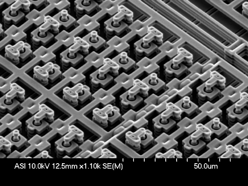
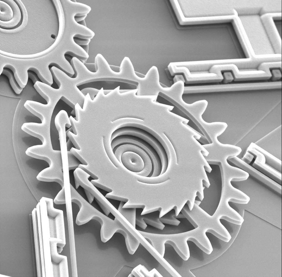
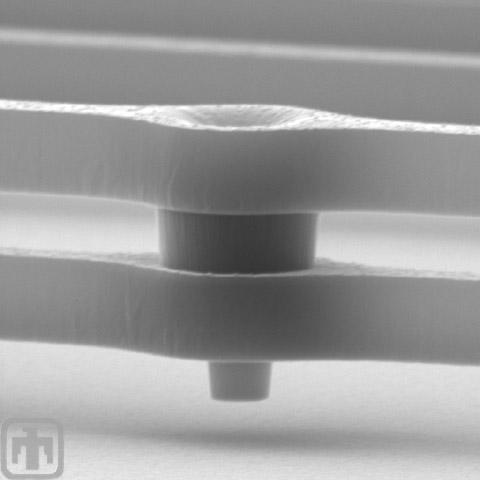
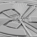
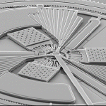
Image of Section of High Performance MEMS Post Actuato


These are the High Performance MEMS Post Actuators.

For more imges please mail me to yaddanapudi1986@yahoo.com

MEMS Applications


Imagine dust, floating in the air, gathering information on the weather, winds, humidity and pollution – all in a tiny cubic millimeter package. This is the “smart dust” scientists at UC Berkeley are developing in the laboratory today. Thousands or millions of these dust motes will sense the environment and communicate simultaneously using MEMS devices. Other applications under development range from such medical uses as hospital rooms that track patients and their medications and treatments, to the use of tiny surgical “scrapers” injected into arteries to clean out plaque, to military reconnaissance, to the detection of biological and chemical weapons.

Automotive: the first high volume application
After spending about 25 years in the lab, however, it was the automotive industry which first commercially embraced MEMS devices in the '90's as airbag accelerometers, recognizing the benefits of MEMS devices' small size, relative low cost and high degree of sensitivity.

Early airbags required the installation of several bulky accelerometers made of discrete components mounted in the front of the car, with separate electronics near the airbag (at a cost of over $50). Today, because of MEMS, the accelerometer and electronics are integrated on a single chip at a cost of under $10. The small size (about the dimensions of a sugar cube) provides a quicker response to rapid deceleration. And because of the very low cost, manufacturers are adding side impact airbags as well. The sensitivity of MEMS devices is also leading to improvements where size and weight of passengers will be calculated so the airbag response will be appropriate for each passenger.

There are many other automotive applications for MEMS either in use now or coming soon, including fuel pressure sensors, air flow sensors, tire pressure sensors with automatic built-in tire pumps, “smart” sensors for collision avoidance and skid detection, “smart” suspension for sport utility vehicles to reduce rollover risk, automatic seatbelt restraint and door locking, vehicle security, headlight leveling, and navigation.

MEMS come of age
Another wide deployment of MEMS is their use as micronozzles that direct the ink in inkjet printers. They are also used to create miniature robots (micro-robots) as well as micro-tweezers, and are used in video projection chips with a million moveable mirrors.

MEMS have been rigorously tested in harsh environments for defense and aerospace where they are used as navigational gyroscopes, sensors for border control and environmental monitoring, and munitions guidance. In medicine they are commonly used in disposable blood pressure transducers and weighing scales.

Out of these practical experiences have grown a raft of other applications which are quickly approaching everyday use. For example, engineers are utilizing the ability of MEMS devices to collectively assemble information and applying it to “smart roads.” Smart roads would be covered with millions of MEMS sensors. The sensors would act as a blanket of information, gathering and transmitting data about road conditions to people charged with maintaining them. Problems with roadways would be detected and repaired before they became serious. These smart roads could also send information to cars equipped with Global Positioning Devices, informing the on-board computer of road hazards, accidents, and traffic. Another safety application includes the detection of black ice on roadways and the development of windshields with automatic glare resistance.

Other arenas into which MEMS are moving include package shipping, where MEMS shock sensors would rest inside packages to monitor time and any type of damage that may occur while the package is in transit. One commercial application that is coming to market within months is a compact skin analysis unit for medical and consumer use, including department store cosmetics counters and pharmacies. This tool will contain small sensor-based units to analyze the physical and chemical properties of skin surfaces.

An additional and significant growth area for MEMS today is in telecommunications where the technology is being used for wireless applications as well as in optical networks.

MEMS Technology-manufacturing techniques


MEMS and ICs: two of a kind
MEMS microstructures are manufactured in batch methodologies similar to computer microchips. The photolithographic techniques that mass-produce millions of complex microchips can also be used simultaneously to develop and produce mechanical sensors and actuators integrated with electronic circuitry. Most MEMS devices are built on wafers of silicon, adopting micromachining technologies from integrated circuit (IC) manufacturing and batch fabrication techniques.

Like ICs, the structures are developed in thin films of materials. The processes are based on depositing thin films of metal or crystalline material on a substrate, applying patterned masks by photolithographic imaging, and then etching the films to the mask. In effect, a sacrificial layer is introduced – a material which keeps other layers separated as the structure is being built up but is dissolved in the very last step allowing selective parts of the structure free to move.

This use of established “batch” processing of MEMS devices, similar to volume IC manufacturing processes, eliminates many of the cost barriers that inhibit large scale production using other less proven technologies. Although MEMS fabrication may consist of a multi-step process, the simultaneous manufacture of large numbers of these devices on a single wafer greatly reduces the overall per unit cost.

Making the transition: from prototype to manufacture
Prototyping is integral to the process, however. An initial device is produced that can be characterized, measured, and optimized for performance and high volume manufacture. A key challenge can be the leap from prototype to high volume manufacture – a transition that sometimes requires considerable modifications. This requires the availability of broad-based design and process expertise (not just application experience), as well as appropriate software tools that can automatically provide process customization. CAD tools are crucial to a cost and time-effective process. Previously developed internally, there are now several commercially available CAD packages that guide engineering teams through component design, system design, and analysis.

It's important to note that MEMS manufacturing technology is not a uniform science but rather a combination of design techniques and knowledge of materials, process, and applications. Processes may vary considerably. For example, the techniques used for wireless may not work at all for the development and production of optical communications devices. Further, although MEMS and IC manufacturing is based on photolithographic etching, in many cases the processes and/or materials may not be compatible. It's interesting to note that gold, which is required in the manufacture of optical MEMS, will contaminate an IC batch.

There are three general approaches to the fabrication of MEMS: surface micromachining, bulk micromachining, and LIGA (lithography, plating, molding).

Surface micromachining is a process based on the building up of material layers selectively remaining or removed by continued processing. The bulk of the substrate remains untouched.

In bulk micromachining, large portions of the substrate are removed to form the desired structure. Structures with greater heights can be formed because thicker substrates can be used. The bulk micromachining process is a key fabrication method used for MEMS-based photonic switching in the high-growth optical and wireless markets.

LIGA processes combine IC lithography and electroplating and molding to obtain depth. Patterns are created in a substrate and then electroplated to create 3D molds. These molds can be used as the final product, or various materials can be injected into them. This process has two advantages. Materials other than silicon can be used (e.g. metal, plastic) and devices with very high aspect ratios can be built.

The fabrication process is usually a structured sequence of THREE BASIC PROCESSES:

1. Deposition
Deposition is a key building block in that it is the ability to deposit thin films of material (for subsequent local etching). MEMS deposition technology is classified in two groups:

Depositions resulting from chemical reactions: chemical vapor deposition, electrodeposition, epitaxy, and themal oxidation. These processes exploit the creation of solid materials directly from chemical reactions in gas and/or liquid compositions or with the substrate material. The solid material is usually not the only product formed by the reaction. Byproducts can include gases, liquids and even other solids.

Depositions resulting from physical reaction: physical vapor deposition, casting. The material deposited is physically moved on to the substrate (a chemical byproduct is not created).

2. Etching
In order to form a functional MEMS structure on a substrate it is necessary to etch the thin films previously deposited and/or the substrate itself. In general, there are two classes of etching processes:

    Wet etchng: the material is dissolved when immersed in a chemical solution
    Dry etching: the material is sputtered or dissolved using reactive ions or a vapor phase etchant.
3. Lithography
Lithography in the MEMS context is typically the transfer of a pattern to a photosensitive material by selective exposure to a radiation source such as light. When a photosensitive material is selectively exposed to radiation (e.g. by masking some of the radiation), the radiation pattern on the material is transferred to the material exposed (the properties of the exposed and unexposed regions differ).


Friday, August 26, 2005

Nano Transistors


A Very Large Scale Integrated (VLSI) circuit is a conglomerate of a large number of practically identical, very reliable switches interconnected to express a computing function. The relentless miniaturization of the components that comprise an Integrated Circuit (IC) which has occurred over the last 30 years has been one of the key ingredients to improving performance while reducing cost by a factor of 100,000. Ultimately, it will become uneconomical to produce reliable transistors through miniaturization, however. The figure shows a cross-section through a 35nm gate length MOSFET, a "nano - transistor", obtained using high resolution Transmission Electron Microscope (TEM). The channel length is only about 100 silicon lattice sites long. An enlargement of the channel region delineated by red on the left is shown on the right. The regular array of atoms show in the lower portion of the lattice image corresponds to the single crystal silicon substrate. The gate oxide thickness estimated from the image is only about 1.0nm. The sensitivity to atomic variables is not welcomed by manufacturing


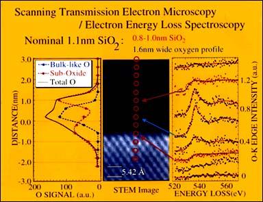
To achieve high performance and high drive current with the low power supply voltage required to minimize power dissipation, the thickness of the gate oxide in sub-100nm CMOS technologies must scale to less than 2nm. However, high resolution Scanning Transmission Electron Microscopy (STEM) used in conjunction with Electron Energy Loss Spectroscopy (EELS) reveals an ultimate physical lower limit to the thickness of about 0.7nm. The figure shows a STEM image of a typical polysilicon/SiO2/silicon gate stack in MOSFET. It shows a regular array of silicon atoms in the substrate, which terminate at the SiO2/Si interface. The chemical constituency of the gate stack and the bonding can be probed by analyzing the energy loss of the transmitted electron beam. We find that a nominally 1.1nm thick oxide has 0.8-1.0nm of bulk SiO2 (blue dashed line) with flanking sub-oxide layers above and below the oxide which are 0.5nm and 0.3nm wide respectively (red dashed line). When the sub-oxide layers coincide, the tunneling barrier associated with the oxide collapses.

Thursday, August 18, 2005

Seminar---Flip Flops

This September 1st I'm going to give a seminar on Flip-Flops.
If any one wanna help me or take help on this related subject please contact me immediately.
Flip-Flops is a basic branch in Digital Design and Communications.
Bye.........Eshwar Prasad

Friday, August 12, 2005

Jokes allround

This time we are gonna see what all the jokes can we collect in this week togather!!
Be ready to get the hot and smooth of all that .Also congratulate tha discovery team for their success.
And at last I request you all to tell me all you know about MEMS/NEMS and free news letters of this.
please do mail me at yaddanapudi1986@gmail.com

Thursday, August 11, 2005

hi

this is eshwar

Sunday, August 07, 2005

Discovery return may it be safe and smooth

Its time that we get our hands togather and pray for God to make the landing of Discovery space shuttle smooth and also to clap for them when they make the landing succeesfully.

Hope we all welcome them with good heart.-----------Eshwar Prasad

Monday, August 01, 2005

NASA space shuttle is scheduled to return on eighth August
The NASA s Discovery space shuttle that is scheduled to come on 7 Aug is now to be on 8th of Aug. to more mail me bbbbbbbbbbbye.