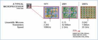
Information technology (IT) is more than a trillion dollar industry. It includes hardware, software, services and applications. Contrary to the perception, the hardware accounts for better than two thirds and the single most important building block of this hardware, of course, is semiconductor devices such as CMOS, Ga -As, Si- Ge, Silicon- on- insulator for a variety of digital, RF, analog and optoelectronic applications. The total worldwide annual market for these devices is about $150 - 200 B. These devices, the technology for which is at the threshold of Nano scale (100nm), are typically fabricated into wafers as big as 300 mm in diameter and are subsequently diced into individual ICs. They are then packaged, tested, and burned into individual IC devices ready to be surface mount bonded onto system level boards. The total number of ICs produced in year 2000 was about 375B units, each packaged at some cost, typically $00.01U.S. per I/O. The total packaging market, which includes IC Packaging as well as system's packaging, is almost as big as the semiconductor market, together accounting for 25% of IT.
No comments:
Post a Comment