MEMS and ICs: two of a kind
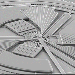
MEMS microstructures are manufactured in batch methodologies similar to computer microchips. The photolithographic techniques that mass-produce millions of complex microchips can also be used simultaneously to develop and produce mechanical sensors and actuators integrated with electronic circuitry. Most MEMS devices are built on wafers of silicon, adopting micromachining technologies from integrated circuit (IC) manufacturing and batch fabrication techniques.
Like ICs, the structures are developed in thin films of materials. The processes are based on depositing thin films of metal or crystalline material on a substrate, applying patterned masks by photolithographic imaging, and then etching the films to the mask. In effect, a sacrificial layer is introduced – a material which keeps other layers separated as the structure is being built up but is dissolved in the very last step allowing selective parts of the structure free to move.
This use of established “batch” processing of MEMS devices, similar to volume IC manufacturing processes, eliminates many of the cost barriers that inhibit large scale production using other less proven technologies. Although MEMS fabrication may consist of a multi-step process, the simultaneous manufacture of large numbers of these devices on a single wafer greatly reduces the overall per unit cost.
Making the transition: from prototype to manufacture
Prototyping is integral to the process, however. An initial device is produced that can be characterized, measured, and optimized for performance and high volume manufacture. A key challenge can be the leap from prototype to high volume manufacture – a transition that sometimes requires considerable modifications. This requires the availability of broad-based design and process expertise (not just application experience), as well as appropriate software tools that can automatically provide process customization. CAD tools are crucial to a cost and time-effective process. Previously developed internally, there are now several commercially available CAD packages that guide engineering teams through component design, system design, and analysis.
It's important to note that MEMS manufacturing technology is not a uniform science but rather a combination of design techniques and knowledge of materials, process, and applications. Processes may vary considerably. For example, the techniques used for wireless may not work at all for the development and production of optical communications devices. Further, although MEMS and IC manufacturing is based on photolithographic etching, in many cases the processes and/or materials may not be compatible. It's interesting to note that gold, which is required in the manufacture of optical MEMS, will contaminate an IC batch.
There are three general approaches to the fabrication of MEMS: surface micromachining, bulk micromachining, and LIGA (lithography, plating, molding).
Surface micromachining is a process based on the building up of material layers selectively remaining or removed by continued processing. The bulk of the substrate remains untouched.
In bulk micromachining, large portions of the substrate are removed to form the desired structure. Structures with greater heights can be formed because thicker substrates can be used. The bulk micromachining process is a key fabrication method used for MEMS-based photonic switching in the high-growth optical and wireless markets.
LIGA processes combine IC lithography and electroplating and molding to obtain depth. Patterns are created in a substrate and then electroplated to create 3D molds. These molds can be used as the final product, or various materials can be injected into them. This process has two advantages. Materials other than silicon can be used (e.g. metal, plastic) and devices with very high aspect ratios can be built.
The fabrication process is usually a structured sequence of THREE BASIC PROCESSES:
1. Deposition
Deposition is a key building block in that it is the ability to deposit thin films of material (for subsequent local etching). MEMS deposition technology is classified in two groups:
Depositions resulting from chemical reactions: chemical vapor deposition, electrodeposition, epitaxy, and themal oxidation. These processes exploit the creation of solid materials directly from chemical reactions in gas and/or liquid compositions or with the substrate material. The solid material is usually not the only product formed by the reaction. Byproducts can include gases, liquids and even other solids.
Depositions resulting from physical reaction: physical vapor deposition, casting. The material deposited is physically moved on to the substrate (a chemical byproduct is not created).
2. Etching
In order to form a functional MEMS structure on a substrate it is necessary to etch the thin films previously deposited and/or the substrate itself. In general, there are two classes of etching processes:
- Wet etchng: the material is dissolved when immersed in a chemical solution
Dry etching: the material is sputtered or dissolved using reactive ions or a vapor phase etchant.
Lithography in the MEMS context is typically the transfer of a pattern to a photosensitive material by selective exposure to a radiation source such as light. When a photosensitive material is selectively exposed to radiation (e.g. by masking some of the radiation), the radiation pattern on the material is transferred to the material exposed (the properties of the exposed and unexposed regions differ).
No comments:
Post a Comment